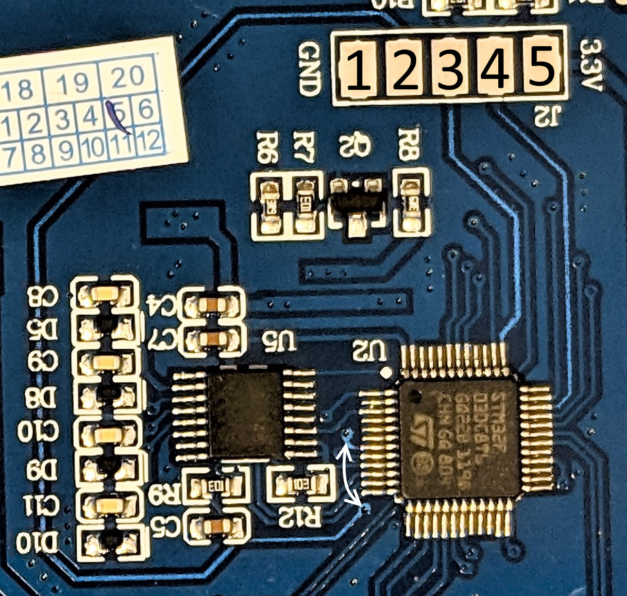
On each TJC/Nextion basic panel is a set of 5 pads labeled J2. Nextion has always been cagey about these pads and tend to delete any posts mentioning them (it’s something of a theme with them). Here’s what they look like:
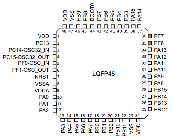
For reference, here’s the STM32
These pads are used to flash the STM32 processor via Serial Wire Debug
Tracing the paths, here’s what we can see:
| 1 | 2 | 3 | 4 | 5 |
|---|---|---|---|---|
| GND | RESET | SWCLK | SWDIO | 3.3V |